Lab 4 - EE 421L
IV Characteristics and Layout of NMOS and PMOS Devices in ON's C5 Process
Authored
by Saied Samara,
Email: Samaras@unlv.Nevada.edu
27 September 2015
Pre Lab:
-For the pre lab work we need to:
- Back-up all of the work from the lab and the course.
- Read through this lab before starting it.
- Go through Tutorial 2.
- In
the simulations in this lab the body of all NMOS devices (the
substrate) should be at gound (gnd!) and the vody of all PMOS devices
(the n-well) should be at a vdd! of 5V.
-------------------------------------------------------------------------------------------------------------------------------------------------------------------------------------------
Post Lab
-Lab Discription:
For the post lab work we need to:
- Generate 4 schematics and simulations of:
- A schematic for simulating ID
v. VDS of an NMOS device for VGS varying from 0 to 5 V in 1 V steps
while VDS varies from 0 to 5 V in 1 mV steps. Use a 6u/600n
width-to-length ratio.
- A
schematic for simulating ID v. VGS of an NMOS device for VDS = 100 mV
where VGS varies from 0 to 2 V in 1 mV steps. Again use a 6u/600n
width-to-length ratio.
- A
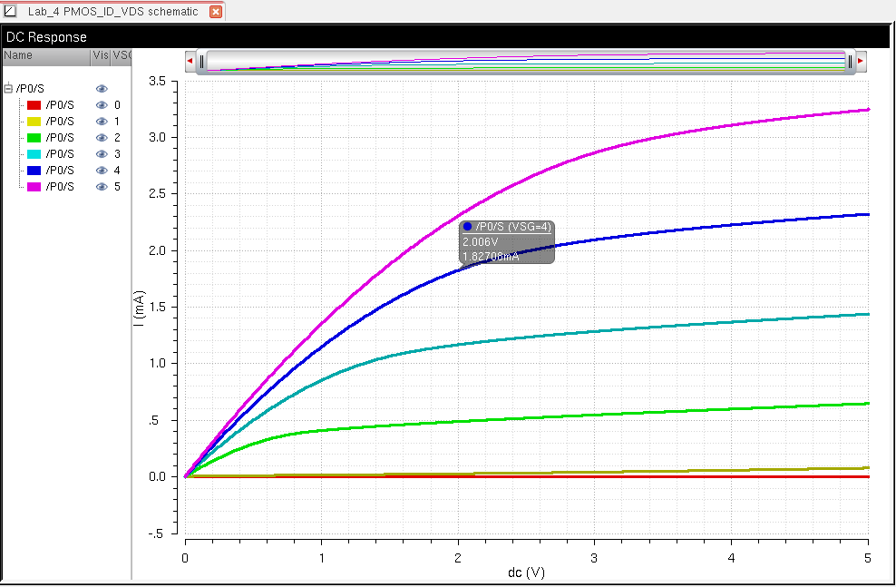
schematic for simulating ID v. VSD (note VSD not VDS) of a PMOS device
for VSG (not VGS) varying from 0 to 5 V in 1 V steps while VSD varies
from 0 to 5 V in 1 mV steps. Use a 12u/600n width-to-length ratio.
- A
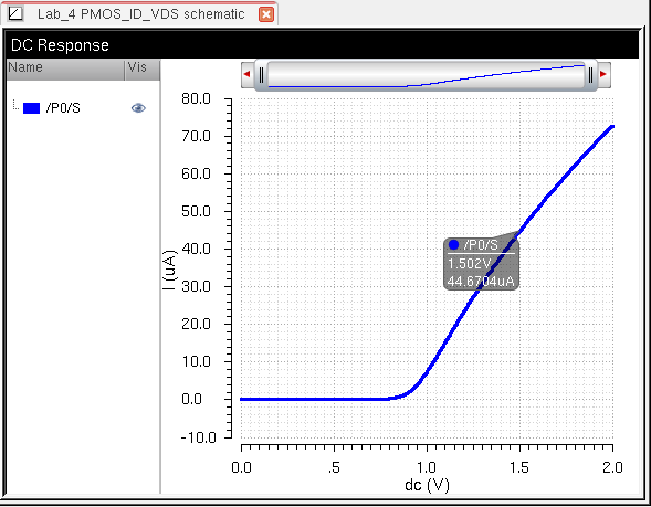
schematic for simulating ID v. VSG of a PMOS device for VSD = 100 mV
where VSG varies from 0 to 2 V in 1 mV steps. Again, use a 12u/600n
width-to-length ratio.
- Lay out a 6u/0.6u NMOS device and connect all 4 MOSFET terminals to probe pads, and directly adjacent to the MOSFET (so the layout is relative small).
- Lay out a 12u/0.6u PMOS device and connect all 4 MOSFET terminals to probe pads.
-> Plot the IV characteristic curves for NMOS and PMOS devices.
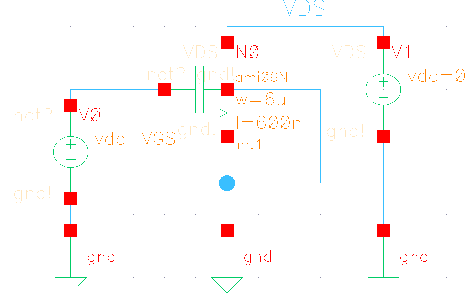
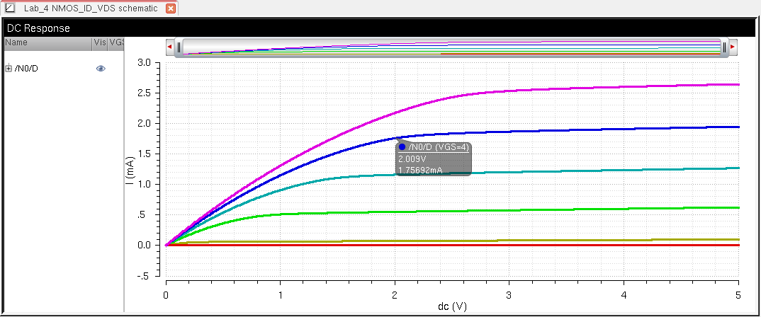
-First designing an NMOS device of 6u/600n, and
simulating ID vs VDS for VGS varying from 0 to 5V, as seen below:
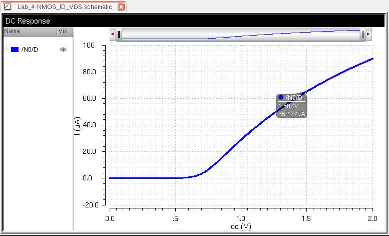
-Simulating ID vs VGS for VDS = 100mV where VGS varies from 0 to 2V as seen below:
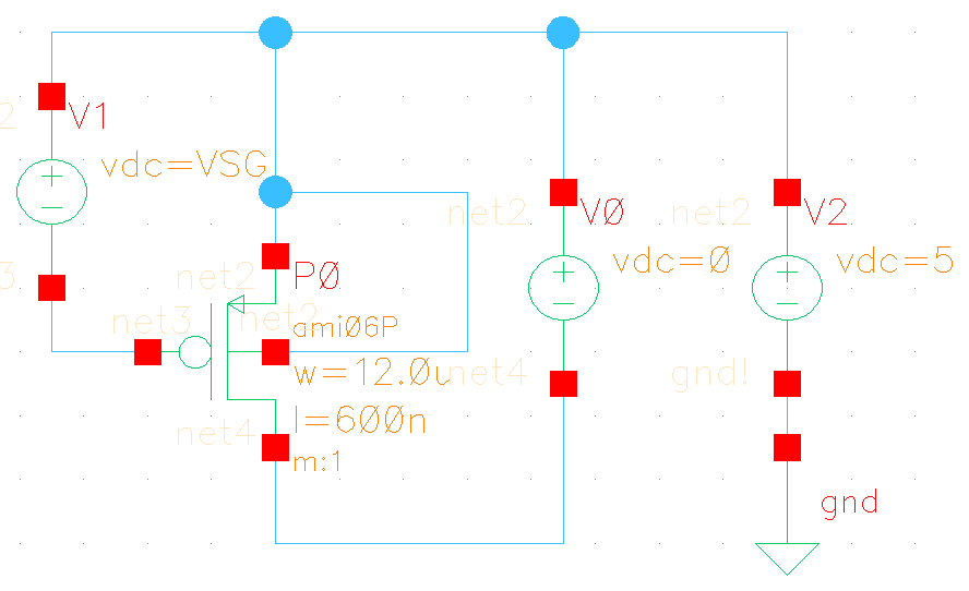
-Next disigning a PMOS device of 12u/600n, and simulating ID vs VSG for
VSG varying from 0 to 5V as seen below:
-Simulating ID vs VSG for VSD = 100mV where VSG varies from 0 to 2V as seen below:
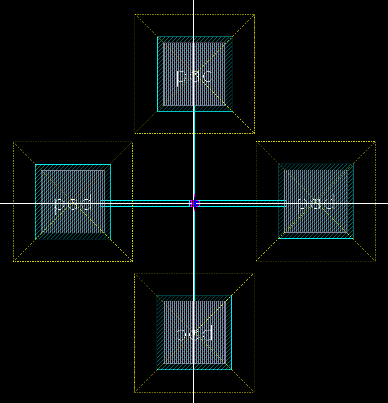
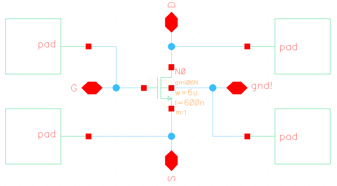
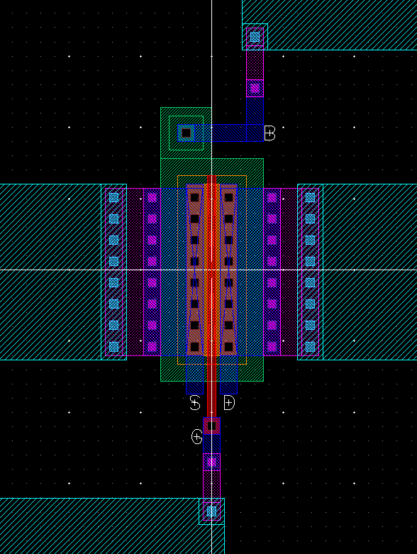
-> Lay out a 6u/0.6u NMOS device and connect all 4 MOSFET terminals to probe pads, as seen below:
-Connecting the NMOS to the pads:
-> Now let us creat a schematic for our NMOS so we can LVS it and verify it
-> Let us start first with the probe-pads, as seen here:
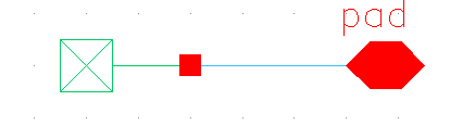 creating a symbol for our pad ->
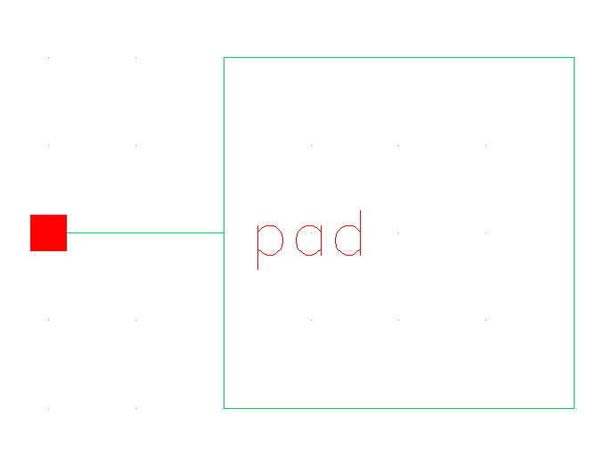
-> NMOS complete schematic, as seen below:
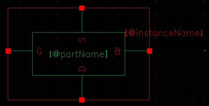
-Creating a symbol for our NMOS device:
*NOTE: here we see that our base pin is denoted as B, but when
perfoming LVS I change it to gnd! to match our NMOS layout.
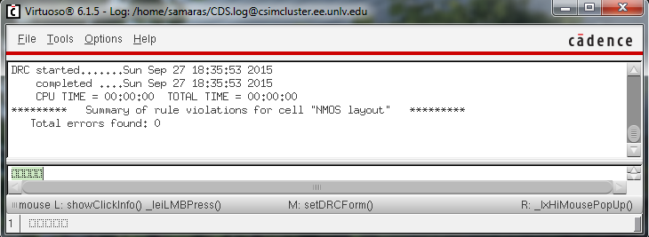
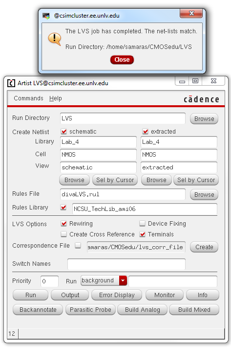
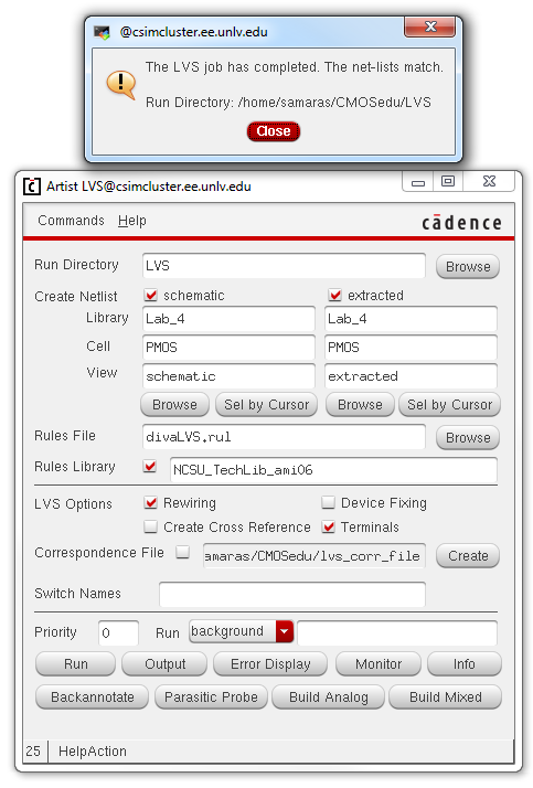
-> Performing LVS to our NMOS device:
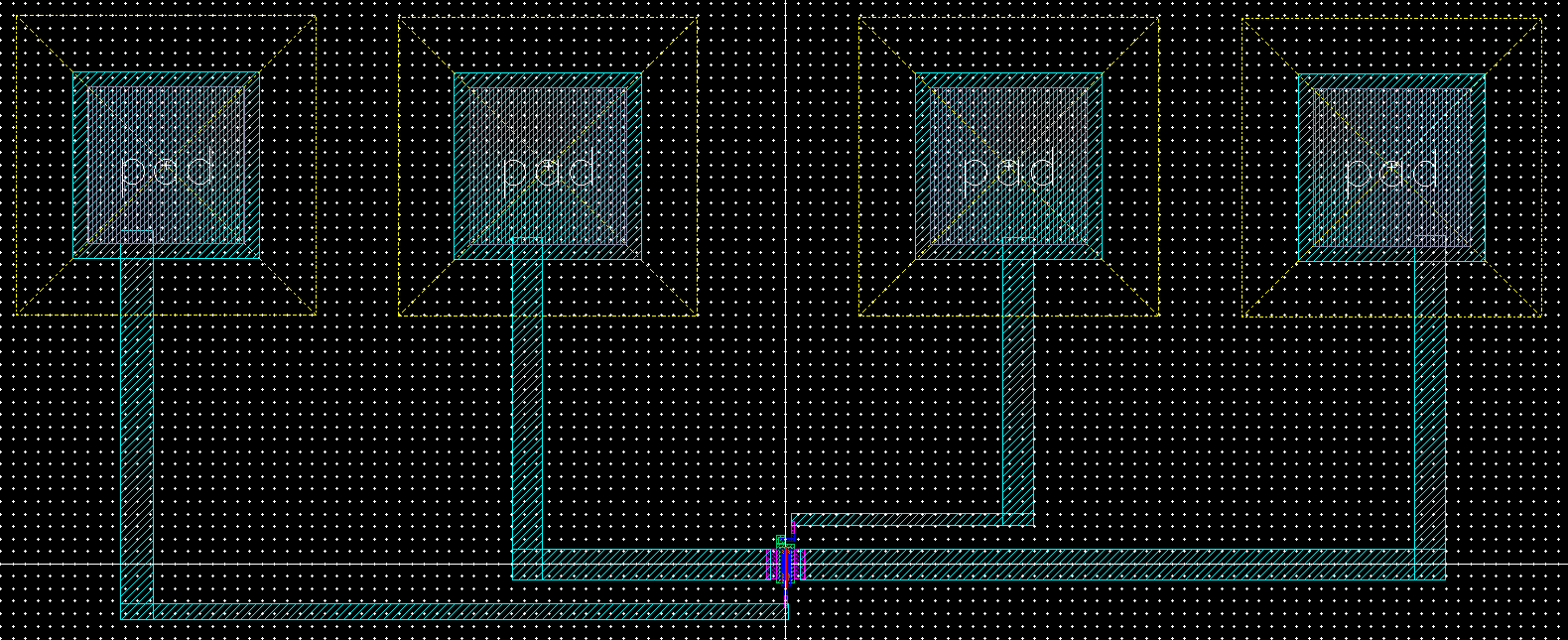
-> Lay out a 12u/0.6u PMOS device and connect all 4 MOSFET terminals to pads, as seen below:
-Connecting the PMOS to the pads:
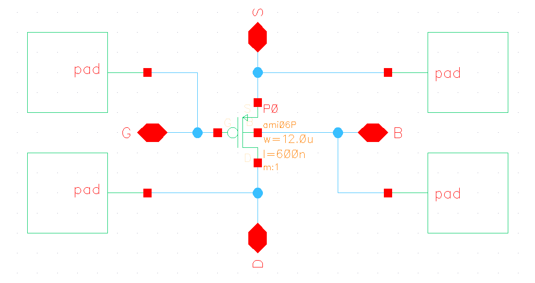
-> Now let us creat a schematic for our PMOS se we can LVS it and verify it.
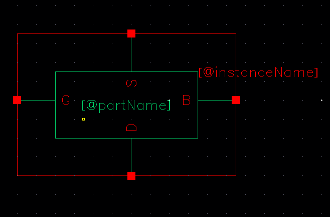
-Creating a symbol for our PMOS device:
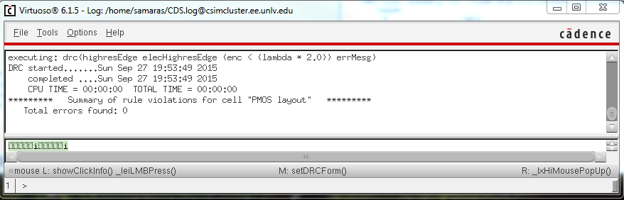
-> Performing LVS to our NMOS device:
-------------------------------------------------------------------------------------------------------------------------------------------------------------------------------------------
-> Backing up:
-------------------------------------------------------------------------------------------------------------------------------------------------------------------------------------------
Return to my EE421L labs
Return to EE421L labs